Note: 빨간색으로 표기된 항목은 U6220A에서 사용할 수 없습니다.
12 Digits 분해능 & 6 GHz 주파수 측정
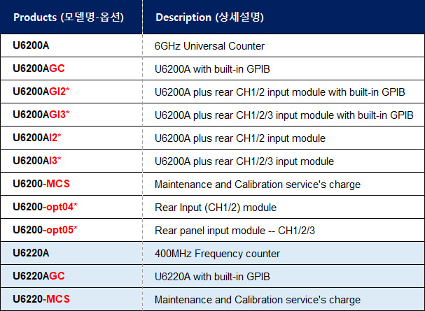
생산 절차가 ISO 9004를 준수하는 Picotest U6200A 범용 카운터는 초당 12자리(그림 1)의 주파수 분해능, 40ps의 시간 간격 분해능 및 테스트와 분석 기능에 적합한 세트 구성입니다. 표준 U6200A의 CH3 범위는 375MHz ~ 6GHz이고 표준 CH 1 및 2 범위는 1mHz ~ 400MHz입니다.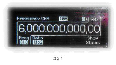
범용성을 위한 뛰어난 기능
Picotest U6200A는 Frequency & Ratio (11Digits/Sec.), Time interval, Period (2.5 ns to 1000s), Duty Cycle, Pulse Width, Rise/Fall Time, Peak Volts (100 Hz~300 MHz), Phase, Totalize, Temperature Stability (< 1 PPM), Aging Rate (< 2 PPM per year), timebase reference channel (Figure-2) and complete Front-End Isolation의 기능을 제공합니다.
Full Math Functions & Easy Operation Panel
U6200A는 실시간 디지털 신호 처리 기술을 지원하여 데이터를 분석하는 동시에 새로운 판독값과 과속 측정값을 얻는 데 적용할 수 있습니다. "Limit Modes"는 탁월한 기능으로, 사용자가 특정한 측정을할 때 마진을 설정할 수 있고, Go-On 또는 Stop 및 USB 출력 설정 을 통해(그림-6), U6200A는 한계를 초과하면 측정을 계속하거나 중지할 수 있습니다.또한 외부 장치를 트리거하는 출력 신호를 생성할 수 있습니다.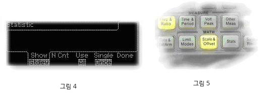
무료 소프트웨어 및 친숙한 SCPI 명령
사용자는 USB 또는 GPIB(Opt) 인터페이스를 사용하여 PC 소프트웨어(Microsoft Excel®)를 통해 데이터 로그(그림 9)를 얻을 수 있습니다. 뿐만 아니라, U6200A는 웹서버 기능도 지원하며, 따라서 사용자는 웹 브라우저에 이더넷 주소(기본값: 192.168.0.247)를 입력하여 LAN 인터페이스(그림 10)를 통해 쉽게 제어할 수 있습니다. 또한 Agilent 53132A와 호환되는 SCPI 명령을 통해 Picotest U6200A는 사용자 애플리케이션에 익숙한 구문 문자열을 활용할 수 있습니다. 자세한 명령 정보는 U6200A 사용 설명서 7장을 참조하십시오.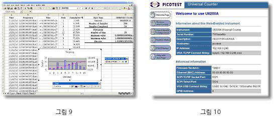
다양한 기능
PDF Download
U6200A / U6220A Specifications
A. Specification List
아래의 내용은 U6200A/220A의 다양한 사양를 표시했습니다. 특히 다양한 조건에서 AC, DC, 저항, 온도 및 주파수/주기를 표기했습니다. 또한 사용자의 편의를 위해 일반적인 특성 및 정확도 계산도 포함되어 있습니다. 이러한 사양은 개발자의 생산 및 엔지니어링 연구 목적에 대한 요구 사항을 충분히 충족할 수 있습니다. 달리 명시되지 않는 한 모든 사양은 U6200A/220A에 포함됩니다.
※ Note: U6220A는 녹색 사양을 제공하지 않습니다. .
|
Channel 1 & 2 (for U6200A only) Input Specifications |
||
|
DC Coupled |
1mHz to 400 MHz |
|
|
AC Coupled |
200KHz to 400 MHz (50 Ω) 30 Hz to 400 MHz (1 MΩ) |
|
|
FM Tolerance |
FM Tolerance: 25% |
|
|
Voltage Range and Sensitivity |
||
|
1mH to 225 MHz |
20 mVrms to ±5 V ac + dc (Medium and High) 25 mVrms to ±5 V ac + dc (Low) |
|
|
225 MHz to 400 MHz |
30 mVrms to ±5 V ac + dc |
|
|
Channel 1 & 2 (for U6200A only) Input Characteristics |
||
|
Impedance (ATT X 1, 1 MΩ Capacitance) (ATT X 10, 1 MΩ Capacitance) |
1 MΩ or 50 Ω 24 pF 15 pF |
|
|
Coupling |
AC or DC |
|
|
Low-Pass Filter |
100 KHz (or disabled) –20 dB at > 1 MHz |
|
|
Input Sensitivity |
Selectable between Low, Medium(default), or High Medium is approximately 1.35x High Sensitivity, low is approximately 1.7x High Sensitivity |
|
|
Internal Noise |
200uVrms(typical) |
|
|
|
||
|
Voltage Range and Sensitivity (Single-Shot Pulse) |
||
|
1.5ns to 10ns Pulse Width |
80 mVpp to 10 Vpp (150 mVpp with optional rear connectors) |
|
|
>10 ns Pulse Width |
50 mVpp to 10 Vpp (150 mVpp with optional rear connectors) |
|
|
|
||
|
Trigger Level(ATT x 1) |
||
|
Range |
±5.125 V |
|
|
Accuracy |
±(15 mV + 1% of trigger level) |
|
|
Resolution |
2.5mV |
|
|
ATT x 10 Range |
X 10 |
|
|
Trigger Slope |
Positive or Negative |
|
|
Auto Trigger Level |
Range |
0 to 100% in 1% steps |
|
Frequency |
Peak Voltage fast mode >10 KHz Peak Voltage slow mode > 100 Hz Amplitude> 100 mVpp (No amplitude modulation) |
|
|
|
||
|
Damage Level |
||
|
DC~400MHz 50 Ω |
12 Vrms |
|
|
0 to 3.5 kHz, 1 MΩ |
350 V dc + ac pk |
|
|
3.5 kHz to 100KHz, 1 MΩ |
350 V dc + ac pk linearly derated to 12 Vrms |
|
|
100KHz to 400MHz, 1 MΩ |
12 Vrms |
|
|
Attenuator |
||
|
Voltage Range |
x10 |
|
|
Trigger Range |
x10 |
|
1. Specifications and Characteristics for Channels 1 and 2 are identical for both Common and Separate Configurations.
2. Values shown are for x 1 attenuator setting. Multiply all values by 10 (nominal) when using the x 10 attenuator setting. Note that it may necessary to recalibrate the input offset in the application environment (especially at high temperature) to achieve maximum sensitivity.
|
|
||||||||||
|
Channel 3 Input Specifications (for U6200A only) |
||||||||||
|
Frequency Range |
375 MHz to 6 GHz |
|||||||||
|
Channel 3 Input Characteristics (for U6200A only) |
||||||||||
|
Impedance |
50 Ω |
|||||||||
|
Coupling |
AC |
|||||||||
|
VSWR |
< 2.5:1 |
|||||||||
|
Power Range and Sensitivity (Sinusoid) |
||||||||||
|
375 MHz to 500 MHz |
-16 dBm to +15 dBm |
|||||||||
|
500 MHz to 1 GHz |
-20 dBm to +15 dBm |
|||||||||
|
1 GHz to 2 GHz |
-23 dBm to +15 dBm |
|||||||||
|
2 GHz to 4 GHz |
-25 dBm to +15 dBm |
|||||||||
|
4 GHz to 5 GHz |
-21dBm to +15 dBm |
|||||||||
|
5 GHz to 5.5 GHz |
-20 dBm to +15 dBm |
|||||||||
|
5.5 GHz to 6 GHz |
-17 dBm to +15 dBm |
|||||||||
|
Damage Level |
||||||||||
|
+25 dBm, DC ±12V |
||||||||||
|
|
||||||||||
|
External Arm Input Specifications |
||||||||||
|
Signal Input Range |
LVTTL and TTL compatible |
|||||||||
|
Timing Restrictions |
||||||||||
|
Pulse Width |
> 50 ns |
|||||||||
|
Transition Time |
< 250 ns |
|||||||||
|
Start-to-Stop Time |
> 50 ns |
|||||||||
|
Damage Level |
12 Vrms |
|||||||||
|
External Arm Input Characteristics |
||||||||||
|
Impedance |
1 kΩ |
|||||||||
|
Input Capacitance |
17 pF |
|||||||||
|
Start Slope |
Positive or Negative |
|||||||||
|
Stop Slope |
Positive or Negative |
|||||||||
|
Notes |
1. External Arm is available for all measurements except Peak Volts. 2. External Arm is referred to as External Gate for some measurements. |
|||||||||
|
|
||||||||||
|
Internal Time Base Stability |
||||||||||
|
|
Standard (0° to 50°C) |
|||||||||
|
Temperature Stability (referenced to 25°C) |
<± 1 x 10⁻⁶ |
|||||||||
|
Aging Rate |
Per Day Per Month Per Year |
± 2 ppm |
||||||||
|
Calibration |
Electronic |
|||||||||
|
|
||||||||||
|
External Time Base Input Specifications |
||||||||||
|
Voltage Range |
200 mVrms to 10 Vrms |
|||||||||
|
Damage Level |
12 Vrms |
|||||||||
|
External Time Base Input Characteristics |
||||||||||
|
Threshold |
0 V |
|||||||||
|
Impedance |
1 kΩ |
|||||||||
|
Input Capacitance |
25 pF |
|||||||||
|
Input Frequency |
10 MHz |
|||||||||
|
Internal vs. External Time Base Selection |
Manual |
Select Internal or External |
||||||||
|
Automatic |
Internal used when External not present (default) |
|||||||||
|
Time Base Output Specifications |
||||||||||
|
Output Frequency |
10 MHz |
|||||||||
|
Voltage |
570 mVpp (0 dBm), typical |
|||||||||
|
Impedance |
50 Ω (typical), AC coupled |
|||||||||
|
|
||||||||||
|
Measurement Specifications |
||||||||||
|
Frequency, Period Channel 1 and 2 |
1 mHz to 400 MHz (2.5 ns to 1000 s) |
|||||||||
|
Trigger |
Default setting is Auto Trigger at 50 % |
|||||||||
|
“Default” Gate Time |
0.1 sec |
|||||||||
|
STD CH 3 |
375 MHz to 6 GHz (0.166 ns to 2.6 ns) |
|||||||||
|
Frequency Ratio |
CH 1/ CH 2, CH 1/ CH 3, CH 2/ CH 1, CH 3/ CH1 |
|||||||||
|
(Measurement is specified over the full signal range of each input.) |
||||||||||
|
Results Range |
10-10 to 1011 |
|||||||||
|
“Default” Gate Time |
0.1 sec |
|||||||||
|
Time Interval |
Measurement is specified over the full signal ranges of Channels 1 and 2. The width of the pulse must be greater than 1 ns, frequency range to 300 MHz. |
|||||||||
|
Trigger |
Default setting is Auto Trigger at 50 % |
|||||||||
|
Results Range |
-0.5 ns to 105 s |
|||||||||
|
Resolution |
40 ps |
|||||||||
|
RMS Resolution |
120 ps |
|||||||||
|
Systematic Uncertainty |
±(TI × Time Base Error) ± Trigger Level Timing Error ± 500 ps Differential Channel Error |
|||||||||
|
Pulse Width Time |
Measurement is specified over the full signal range of Channel 1. The width of the pulse must be greater than 1 ns frequency range to 300 MHz). |
|||||||||
|
Pulse Selection |
Positive or Negative |
|||||||||
|
Trigger |
Default setting is Auto Trigger at 50% |
|||||||||
|
Results Range |
1.5 ns to 105 s |
|||||||||
|
Resolution |
40 ps |
|||||||||
|
RMS Resolution |
120 ps |
|||||||||
|
Systematic Uncertainty |
± (Pulse Width Time x Time Base Error) ± Trigger Level Timing Error ± 500 ps Differential Channel Error. |
|||||||||
|
Rise/Fall Time |
Measurement is specified over the full signal range of Channel 1. The width of the pulse must be greater than 1 ns frequency range to 300 MHz). |
|||||||||
|
Edge Selection |
Positive or Negative |
|||||||||
|
Trigger |
Default setting is Auto Trigger at 10% and 90% |
|||||||||
|
Results Range |
2 ns to 105 s |
|||||||||
|
Resolution |
40 ps |
|||||||||
|
RMS Resolution |
120 ps |
|||||||||
|
Systematic Uncertainty |
± (Edge Time x Time Base Error) ± Trigger Level Timing Error ± 500 ps Differential Channel Error |
|||||||||
|
Phase |
Measurement is specified over the full signal range of each input. The width of the pulse must be greater than 1 ns, frequency range to 300 MHz |
|||||||||
|
Results Range |
-180° to +360° |
|||||||||
|
Resolution |
40 ps |
|||||||||
|
RMS Resolution |
120 ps |
|||||||||
|
Systematic Uncertainty |
± (Trigger Level Timing Error) ×Frequency |
|||||||||
|
Duty Cycle |
Measurement is specified over the full signal range of Channel 1. The width of the pulse must be greater than 1 ns, frequency range to 300 MHz |
|||||||||
|
Pulse Selection |
Positive or Negative |
|||||||||
|
Trigger |
Default setting is Auto Trigger at 50 % |
|||||||||
|
Results Range |
0 to 1 |
|||||||||
|
Resolution |
40 ps |
|||||||||
|
RMS Resolution |
120 ps |
|||||||||
|
SystematicUncertainty |
± Trigger Level Timing Error ± 500 ps Differential Channel Error |
|||||||||
|
Totalize |
Measurement is specified over the full signal range of Channel 1. The width of the pulse must be greater than 1 ns, frequency range to 400 MHz |
|||||||||
|
Pulse Selection |
Positive or Negative |
|||||||||
|
Trigger |
Default setting is Trigger at 0 V |
|||||||||
|
Results Range |
0 to 1015 |
|||||||||
|
Resolution |
1 count |
|||||||||
|
Systematic Uncertainty |
± 1 count |
|||||||||
|
Peak Voltage |
Results Range |
-5.1 V to + 5.1 V | ||||||||
|
Resolution |
2.5 mV | |||||||||
|
DC Signals |
|
15 mV + 2 % of V | peak-to-peak amplitude greater than 200 mV | |||||||
|
DC Signals (ATT x 10) |
|
150 mV + 2 % of V | peak-to-peak amplitude greater than 1 V | |||||||
|
1 Vp-p, 50 Ω, ATT OFF |
100 Hz ~ 10 KHz |
15 mV + 2 % of V |
peak-to-peak amplitude greater than 200 mV | |||||||
|
10 KHz ~ 5 MHz |
15 mV + 4 % of V |
|||||||||
|
5 MHz ~ 80 MHz |
15 mV + 7 % of V |
|||||||||
|
80 MHz ~ 300 MHz |
15 mV + 15 % of V |
|||||||||
|
|
||||||||||
|
Rear Input Option Channel Isolation |
||||||||||
|
Frequency |
Front Channel(dB) |
Rear Channel(dB) |
||||||||
|
100KHz |
<-85 |
<-85 |
||||||||
|
1MHz |
-85 |
-75 |
||||||||
|
10MHz |
-78 |
-55 |
||||||||
|
50MHz |
-67 |
-42 |
||||||||
|
100MHz |
-62 |
-37 |
||||||||
|
200MHz |
-55 |
-35 |
||||||||
|
300MHz |
-50 |
-36 |
||||||||
|
400MHz |
-47 |
-33 |
||||||||
The peak volts measurement will keep operating up to 400 MHz, although results act as references only.
The differential channel Error terms which counted by many systematic uncertainty equations result channel-to-channel disaccord and internal noise. These issues can be improved by the TI calibration in the well-controlled temperature environment.
A.1 RMS Resolution
|
Rms |
100Hz |
1KHz |
10KHz |
100KHz |
|
U62 (10ms) |
0.000000842 |
0.000003438 |
0.000013896 |
0.000067275 |
|
U62 (100ms) |
0.0000001 |
0.000000828 |
0.000005093 |
0.000011508 |
|
U62 (1s) |
0.000000001 |
0.000000098 |
0.000001212 |
0.000004869 |
|
Rms |
1MHz |
10MHz |
100MHz |
1GHz |
|
U62 (10ms) |
0.000677504 |
0.004830870 |
0.042107484 |
0.611551072 |
|
U62 (100ms) |
0.000101040 |
0.002272900 |
0.006344503 |
0.055991810 |
|
U62 (1s) |
0.000058166 |
0.000469601 |
0.001275299 |
0.002602258 |
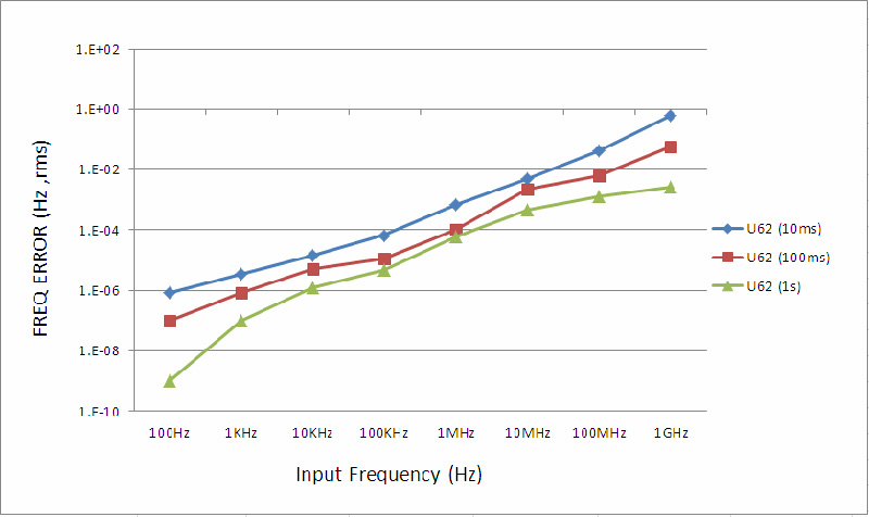
The graph doesn’t include the effects of trigger error. To place an upper bound on the added effect of this error term, it’s necessary to determine the frequency error from the proper graph and add a trigger error term as the following equation:

External source and input amplifier noise might advance or postpone the trigger points that define the start and end of a measurement. The resulting timing uncertainty is a function of the slew rate of the signal and the amplitude of spurious noise spikes (relative to the input hysteresis band).
The (rms) trigger error relative to a single trigger point is:

B. Preset Values and Save/Recall Information
※ Note: The U6220A doesn’t provide the function via the channel 2 colored green.
|
|
Value at *RST |
In Save/Recal |
In non-volatile memory |
|
|
Input impedance |
CH1 |
1E+6Ohms |
yes |
no |
|
CH2 |
1E+6Ohms |
yes |
no |
|
|
Input Attenuation |
CH1 |
×1 |
yes |
no |
|
CH2 |
×1 |
yes |
no |
|
|
Trigger Level |
CH1 (percent) |
50 |
yes |
no |
|
CH2 (percent) |
50 |
yes |
no |
|
|
CH1 (volts) |
0 |
yes |
no |
|
|
CH2 (volts) |
0 |
yes |
no |
|
|
Trigger Slope |
CH1 |
positive |
yes |
no |
|
CH2 |
positive |
yes |
no |
|
|
Sensitivity |
CH1 |
Medium |
yes |
no |
|
CH2 |
Medium |
yes |
no |
|
|
Scale |
1 |
yes |
no |
|
|
Offset |
0 |
yes |
no |
|
|
Limits parameters |
Limit test on/off |
off |
yes |
no |
|
On fail stop/go on |
go on |
yes |
no |
|
|
Lower limit |
0 |
yes |
no |
|
|
Upper Limit |
0 |
yes |
no |
|
|
Stats parameters |
Stats on/off |
off |
yes |
no |
|
Measurement count |
100 |
yes |
no |
|
|
Display measurement/stats |
measurement |
yes |
no |
|
|
Use all/in limits |
all |
yes |
no |
|
|
On-single measurement |
1 |
yes |
no |
|
|
Timebase |
auto |
yes |
no |
|
|
Trigger Offset Cal Parameters |
Channel 1 trigger offset Inp1 cal |
no |
yes |
|
|
Channel 2 trigger offset Inp2 cal |
no |
yes |
||
|
Channel 1 trigger offset Att1 cal |
no |
yes |
||
|
Channel 2 trigger offset Att2 cal |
no |
yes |
||
|
Trigger Gain Cal Parameters |
Channel 1 trigger gain Inp1 cal |
no |
yes |
|
|
Channel 2 trigger gain Inp2 cal |
no |
yes |
||
|
Channel 1 trigger gain Att1 cal |
no |
yes |
||
|
Channel 2 trigger gain Att2 cal |
no |
yes |
||
|
Time Interval Offset Cal Parameters |
Fine1 |
no |
yes |
|
|
Fine2 |
no |
yes |
||
|
Quick |
no |
yes |
||
|
Timebase cal Parameters |
no |
yes |
||
C. General Specifications
※ Note: The U6220A doesn’t support the accessories from item 1 ~ 4 colored green.
| Item | Limitation & description |
| Power Supply Voltage | 100V/240V ± 10% 50Hz~60Hz ± 10% |
| 100V/120V ± 10% 400Hz ± 10% | |
| Power Requirements | Max. 80VA (30W Typtical) |
| Operating Humidity | Maximum relative humidity 80% for temperature up to 31 ℃ decreasing linearly to 50% relative humidity at 40℃ |
| Operating Environment | 0 to 55 ℃ |
| Storage Temperature | - 40 ℃ to 70 ℃ |
| Operating Altitude | Up to 2000m |
| Dimensions for Rack (WxHxD) | 214.6 x 88.6 x 346.9 mm |
| Weight | 3130 g / 2887 g |
| Safety | IEC61010-1:2010/EN61010-1:2010 (3rd Edition) |
| IEC61010-2-030:2010(1st Edition)/ | |
| EN61010-2-030:2010 | |
| EMC | EN61326, IEC61000-3, IEC61000-4 |
| Warm-up Time | 1 Hour |
| Warranty | 1 Year |
| Accessory |
1. U6200-opt04: Rear panel input module (CH1/CH2) 2. U6200-opt05: Rear panel input module (CH1/CH2/CH3) 3. M3500-opt04: GPIB Card |
※ Note 1: The accessories have to be assembled in Picotest.
※ Note 2: Not to position the equipment so that it is difficult to operate the disconnecting device.
※ Note 3: Documentation shall instruct against replacing detachable mains supply cords by inadequately rated cords.
Universal Counter/ Frequency Counter 주문정보